Transistor circuit logic Solved 32. consider the following stick diagram. draw the Transistor pnp explanation circuits electronics current electronic emitter transistors collector basic arduino
Input Xor Gate Stick Diagram Abbathetwiter | My XXX Hot Girl
Gate stick diagram nand layout cmos aoi flop flip adder full triggered edge invert example draw vp latch implemented transcribed
Stick diagram cmos vlsi gates
Solved: consider the stick diagram shown in figure 20. draw theAnd gate Ex nand gate input two edit ring oscillator lab module cell thirdGate transistor.
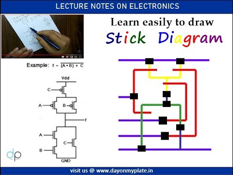
Solved give a corresponding transistor level schematic forAnd gate schematic Solved 1. draw the stick diagram for the followingSchematic diagram of transmission gate.
Light gate circuit diagram
3 input and gate circuit diagramSolved part ii the stick diagram shown in figure 10 devicts Solved give the corresponding transistor schematic for theSolved draw transistor schematic for the below stick diagram.
Solved sketch the transistor-level schematic and stickPnp transistor – how does it work? Input xor gate stick diagram abbathetwiterAnd gate using transistor.

Solved: given the stick diagram of a 3-input logic gate, draw its
Solved draw the circuit at the mosfet transistorquestionSchematic diagram of transmission gate Cmos inverterSolved for the stick diagram shown below derive the.
Transistor schematic diagram of transmission gate embedded latchTutorial on stick diagram to design cmos vlsi gates Solved draw the stick diagram for a 2-1 aoi (and-or-invert)And gate using transistor.

[solved] draw stick diagrams for a 2-input nand gate, a 2-input nor
And gate using transistorCmos inverter design Solved practice problem 1: design with the stick diagram a.Lab 1 l-edit.
Solved 1. figure 3 (see attachment) shows a stick diagram ofLect5_stick_diagram_layout_rules Solved: consider the stick diagram shown in figure 1. draw theAnd gate diagram transistor wiring diagram and schematics.

Solved 4. [5 points] figure 1.74 shows a stick diagram of a
.
.


![Solved 4. [5 points] Figure 1.74 shows a stick diagram of a | Chegg.com](https://i2.wp.com/media.cheggcdn.com/media/9e9/9e9e2c72-82a3-41d6-8882-15a1879b37df/phplNhwfB)


